Words by Paul Willis
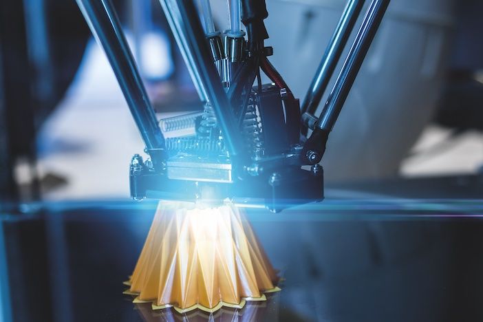
Additive manufacturing, also known as 3D printing, is occupying a growing role in manufacturing. A study published last November for example found that most manufacturing companies (81%) had doubled their use of large-scale additive manufacturing in the previous 12 months.
The study commissioned by the additive manufacturing (AM) technology company Essentium also found that 88% of manufacturers are now using hybrid production, integrating both 3D printed parts and traditionally manufactured parts in the same products.
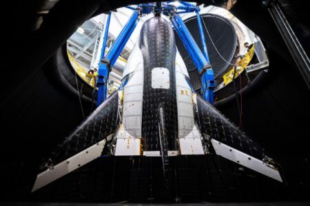
This trend is particularly relevant for the aerospace sector, with industry leaders like BAE Systems widely employing AM. The company set itself the target in 2020 of manufacturing 30% of the next generation Tempest fighter jet using AM.
The main advantage AM offers over subtractive manufacturing techniques is its incredible versatility, says Kevin Pickup, a lead technologist for product verification for BAE Systems Air Sector.
“Not all our customers are going to want exactly the same specification of aircraft,” says Pickup. “So we might need to tweak and change.”
Applying these minor adjustments with traditional forging methods can be a lengthy and costly process. Yet with the use of AM processes like wire arc additive manufacturing or hot isostatic pressing “we can rapidly shorten lead times to market and increase our part variability without the extra costs and long lead time that a forging solution would incur,” says Pickup.
Inspection challenges
Despite these advantages the shift to AM brings its own challenges. Foremost among them is inspection. At present the main method of inspection for aerospace parts is non-destructive testing (NDT), a term which covers several analysis techniques that allow a component to be inspected without damaging it.
Many of these techniques rely on technology that originated in the medical industry for the remote scanning of the human body, such as 2D digital x-ray, ultrasound and computed tomography (CT). But applying these NDT techniques to aerospace parts produced through AM can be challenging because existing NDT techniques have been developed and designed around the subtractive method of manufacture and the associated defect set. Pickup illustrates this point by using the example of a metallic frame that has been machined from a billet – a section of metal used for rolling into bars, rods and sections.
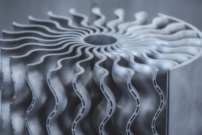
“Before the machine even touched the part, the billet would have been inspected at the metal mill using a traditional ultrasonic method, and that ultrasonic method was designed around the defects that could occur within that particular manufacturing process to up to that point,” says Pickup.
Since each AM method has its own distinct features and defects, successful NDT inspection requires a clear understanding of “where the boundary lies between what is a feature inherent to the process – and what is a defect,” says Pickup.
For example, the additive manufacturing method of friction stir welding is known for creating a fusion defect called a cold lap. “But is that a defect or is it actually something you need to design around because it will always be there?” asks Pickup.
Another challenge for NDT inspection is the complexity of parts that can be produced through AM. 3D printing techniques have allowed aerospace manufacturers to make things they have never been able to make before using subtractive methods such as non-line of sight features and enclosed volumes.
But this complexity makes some areas of the part inaccessible to most inspection tools and methods. The size of the manufactured part can also cause issues for the inspection process. “The deeper you go into a part the harder it is to achieve a certain resolution with an acceptable level of confidence,” says Pickup.
See-through surfboards
One answer to the problems of complexity and scale is to use a much more powerful scanning tool. This approach is used by several NDT companies, including Waygate Technologies, which has built a massive industrial CT scanner at its facility in Cincinnati, USA. The underlying technology of the scanner comes from the medical industry, with the 9MeV linear accelerator scanner based on the linear accelerators used to treat cancer patients.
The machine is housed inside a huge concrete bunker that is large enough to accommodate a car according to Tomas Zikmund, a researcher at the EU-funded Central European Institute of Technology (CEITEC), which has tested the capabilities of Waygate’s scanner in a recent feasibility study.
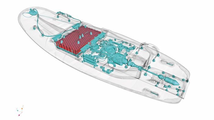
Zikmund and his team partnered with the Czech tech company MSR Engines, which makes motorized surfboards. One of MSR’s Jetsurf surfboards was shipped to Cincinnati and scanned with Waygate’s scanner, known as the Phoenix Power scan HE CT system.
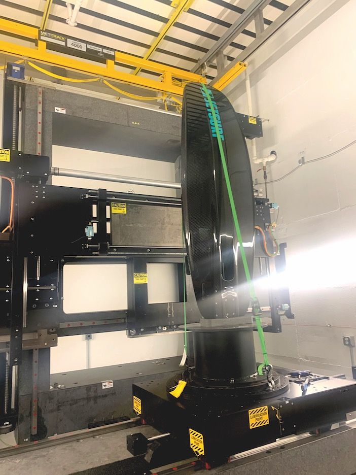
motorized surfboard
Over 30 hours, the board was completely digitized within nine partial scans using a voxel resolution of 150µm. A 250GB data file generated by the scanning was then analyzed at CEITEC’s lab in Brno in the Czech Republic to create a 3D image of the inside of the surfboard.
Zikmund and his team were surprised at the high granularity of the image produced. “We didn’t know what we would get,” said Zikmund. “But we were able to see nearly all the materials.”
This included being able to see within the neoprene used on the board’s surface and inside the board’s propulsion system. Zikmund believes that there are obvious use cases for the linear accelerator in aerospace manufacturing since the high cost of scans make it more likely to be used in special cases where the component being examined is mission critical, as is the case with some aircraft parts.
The scanner’s extremely high voltage also allows it to penetrate inside materials that would ordinarily be too dense for standard CT scanners. Zikmund hopes to eventually bring the technology to Europe. It would be suitable for use testing the Inconel family of nickel and chromium-based superalloys, which are used in aircraft components like turbine rotor blades.
Software solutions
US researcher Amir Ziabari has also devised a novel solution for the inspection of denser alloys like Inconel.
Ziabari began developing algorithms for CT scanners as a post-doctoral researcher at Purdue University in Indiana, later continuing as a scientist at the U.S. Department of Energy’s Oak Ridge National Laboratory.
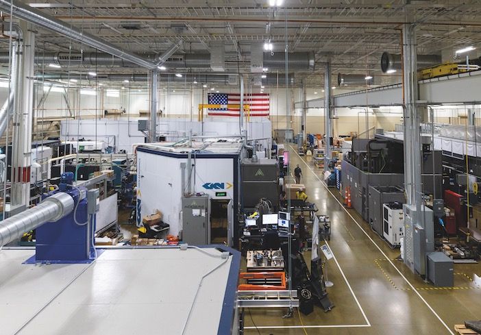
The medical imaging technology he was using was fast but lacked accuracy. During his research, he developed iterative approaches which involve post-process analysis to clean-up the data and eliminate inaccuracies.
While these methods led to far more accurate scans, they were much more time and labor intensive. Ziabari set himself the challenge of developing a NDT process that was as accurate as the iterative approaches, but which could be conducted as quickly and as inexpensively as standard approaches.
The solution he found uses a deep-learning framework to train an algorithm to upgrade low quality data to a higher grade of accuracy. Recognizing its potential application for industry, Ziabari has continued developing the technology for use in NDT inspection of AM parts.
(Image: Brittany Cramer/ORNL, US Dept. of Energy)
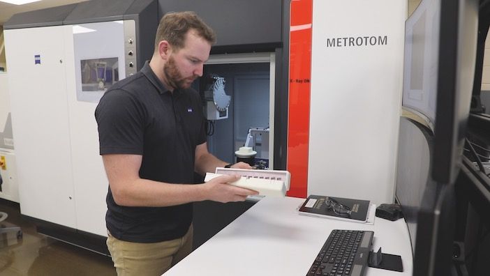
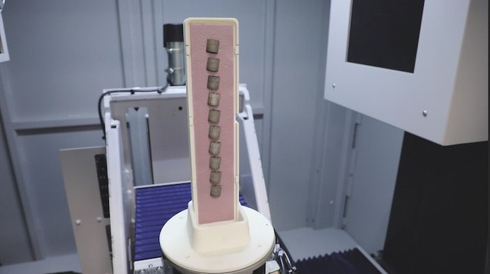
Ziabari and his team have incorporated the framework into software used inside NDT inspection technology developed by the German industrial technology company Zeiss. In collaboration with Zeiss he designed an experiment to test a component that features both simple and complex geometry.
The experiments proved both the accuracy of the deep-learning framework and its speed, with the scan time for the parts made from Inconel alloys improved by up to a factor of six. Ziabari believes his technology could be a valuable tool for aerospace manufacturers that are hoping to reduce the cost and development time of their products.
In-process monitoring
With the same goal in mind, BAE Systems is looking into AM technology that can analyze the quality of a part while it is being printed. In-process monitoring involves collecting all the datasets associated with the 3D printing process as it is happening.
“In the case of friction stir welding for example this would involve collecting data from the different loads on the tool, probably in multiple directions, the speed of rotation, the temperature, the forward velocity and the force applied to the part,” says Pickup.
The result of this data collection would be “a 3D dataset showing how that part has been built that we can compare against baseline values to see whether there would be areas that would require a higher fidelity inspection,” says Pickup.
Since the sheer volume of the data collected by the in-process monitoring would be too much for human analysis, an AI algorithm is required to process the data.
However, inspection engineers need to be careful about this analysis, says Pickup. It needs to be a trusted AI, meaning that the engineers that are using the technology must be able to understand how the AI makes its decisions. Inspection engineers need to be able to prove to a legal standard how a particular aircraft part was qualified for flight “and some of the AI methods don’t really allow us to do that.”
NDT techniques used in aerospace
Several different non-destructive testing (NDT) technologies are commonly used in aerospace development, manufacturing and testing.
Ultrasonics is one of the most common methods and involves the use of transducers to bounce
high-frequency sound waves against a material. This testing technique can be used to identify cracks, weld grooves and fractures, indicate material thickness and moving components.
Radiographic inspection techniques use x-rays or gamma rays to scan a part and can be considered as a complementary inspection technology to ultrasound. This is because radiographic testing can detect volumetric defects that an ultrasonic inspection might miss. It is used primarily to identify flaws in weld quality, castings, structures and composites.
Computed tomography, better known as a CT scan is a form of scanning that combines x-rays with computer processing to create detailed 360˚ views of the interior of a component. In aerospace, it is normally used to inspect smaller components such as turbine blades, aluminum castings and tube welds.
Eddy current testing is particularly useful in the analysis of metallic structures and can used to identify cracking in the surface of aircraft fuselages. The technology uses electromagnetic induction to detect and characterize surface and sub-surface flaws in conductive materials. It works by placing a probe near the surface of the test material. In the probe, an alternating current flows through a wire coil and generates an oscillating magnetic field.


